TiO2 Crystalline Structure “À la Carte”
The featured image was bought on Istock.com and is protected by copyrights.
Abstract Titanium dioxide is a versatile ceramic material possessing applications in several fields that include water cleaning, energy production and transformation and surface modifications. All these applications of TiO2 stem from its unique optoelectronic properties, which strongly depend on the crystalline structure. From research to industrial applications, the ability to include thin layers of crystalline TiO2 without involving high temperature or additional chemical processes is an essential requirement to expand its uses to additive manufacturing and the emerging 4.0 Industrial Revolution.
Ceramics through Soft Chemistry
Ceramics have been around for thousands of years, and they have plenty of technological uses. They are traditionally produced in laboratory and at industrial scale by making powders react at high temperatures above 1000C. In nature, diatoms—unicellular microorganisms—can produce protective ceramic shells at ambient temperatures, in humid environments like the ocean using the silica dissolved in the water. This process, called “soft chemistry”, requires far less energy than the processes involving high temperatures.

Figure 1. Different ceramic shells produced by diatoms
These days, we can produce ceramics at room temperature using sol-gel chemistry, which originates in soft chemistry. The process has been widely used in industry to produce powders and coatings. One well-known example of this is the European Patent House in Frankfurt, whose windows have a sol-gel architectural coating. The coating controls transmission and absorption of different light wavelengths to give a uniform reflective appearance that is aesthetically pleasing, while also mitigating the building’s “greenhouse effect” and reducing cooling costs during the summer.
Combining two Crystalline Structures to Enhance Properties
In the semiconductor field, the use of ceramics is linked to their optoelectronic properties. Ceramic optoelectronic properties change according to their crystalline structure. Titanium dioxide (TiO2) is a remarkable semiconductor with unique optoelectronic properties[1], ideal for photovoltaics and photocatalytic conversion, and possesses more than two crystalline structures, the most popular being anatase and rutile.
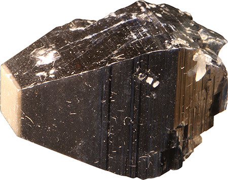
Figure 2 Anatase crystal as it is found in nature
Anatase is mostly used as a blocking layer for optoelectronic or photovoltaic devices, thanks to its wide 3.2eV band gap[2]. Rutile, on the other hand, has a lower electronic band gap of 3.0 eV and is better suited for photoelectrochemical applications[3]. Moreover, combining anatase and rutile has positive consequences on these properties[4], [5]. In the last couple of years, we began reflecting on what could possibly be achieved if mixing crystalline phases could be spatially engineered to effectively control this synergism between anatase and rutile. The next obvious question was How?
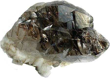
Figure 3 Rutile crystal as it is found in nature
To achieve crystallinity and the desired optoelectronic properties starting from amorphous TiO2, it is necessary to use temperatures above 500C for anatase and above 800C for rutile[6]. However, high-temperature crystallization yields either anatase or rutile and limits their combined use. As such, the high temperatures used to reach anatase and rutile can also be quite detrimental to temperature-sensitive devices. Given the wide range of possibilities that TiO2 has to offer in the development of new flexible, lightweight and wearable technologies requiring low-temperature substrates, researchers have tried to crystallize TiO2 before its integration into devices. This approach partially succeeded in avoiding high-temperature crystallization but the degree of crystallinity and the optoelectronic properties of the resulting TiO2 are far from ideal[7]. Other approaches use low intensity laser irradiation of TiO2 powders under vacuum[8] or Fe and Al-doped TiO2 nanoparticles under oxygen-poor conditions to optically induce crystallization[9]. These methods completely avoid high temperatures but the use of vacuum and the lack of precise control for film micropatterning makes them far from being industrially attractive and compatible with the emerging 4.0 Industrial Revolution.
Proposed Method
In this perspective, it seems that achieving high-quality crystalline TiO2 at room conditions remains one of today’s most important technical challenges towards low-cost optoelectronic devices. In response to this, we devised a much simpler method based on sol-gel chemistry to produce an ink of amorphous TiO2 nanoparticles (10nm) that are rich in oxygen vacancies (defects). As a consequence of the high concentration of defects, films created using our amorphous TiO2 ink can absorb energy in the form of light instead temperature and can be crystallized into anatase and rutile at room temperature and ambient air using laser irradiation.

Figure 4 Patterning of crystalline structure “à la carte”
In the same way that controlling the temperature yields anatase (500C) or rutile (800C), in our process we control and pattern a crystalline structure over amorphous TiO2 films simply by adjusting the power density of the laser. Crystallization occurs after 6s of irradiation and Raman spectroscopy is used to confirm the crystallinity of the films. What is even more remarkable is that anatase and rutile are no longer mutually exclusive and can be patterned one next to the other. This brings the possibility of exploring the synergism between anatase and rutile. In fact, we are currently working on patterning anatase and rutile in much larger areas in the order of mm2 using a low-cost commercial laser-engraving setup (BIBO 3D printer). Our ultimate goal is to automate the crystallization process and merge our high-quality crystalline TiO2 films with the flexible printed electronics technology.
Conclusion
We believe this accurate, reproducible, and industrial scalable method of producing crystalline TiO2 opens the door to novel pathways of TiO2-based platforms, especially for energy conversion, storage and environmental applications. Perhaps we are not yet at the level of diatoms to produce ceramics in such an efficient fashion, but we are getting closer by using the transformational power of nanotechnology.

Figure 5 Crystalline structure “à la carte”. Left: ÉTS pattern logo over amorphous TiO2 film. Right: Anatase and rutile patterned areas and Raman spectra. The blue and red colors represent anatase and rutile, respectively.
Additional Information
For more information on this research, please read the following paper: Benavides, J.A.; Trudeau, C.P.; Gerlein, L.P.; Cloutier, S.G. 2018. Laser Selective Photoactivation of Amorphous TiO2 Films to Anatase and/or Rutile Crystalline Phases. ACS Appl. Energy Mater. 1, 8, 3607-3613.