Light-Sensitive Titanium Dioxide for Printed Electronics
The header image is the property of the authors. CC license.
Until now, use of solution-based titanium dioxide (TiO2) in optoelectronics has been elusive due to its high processing temperature required for crystallization. This limits compatibility with temperature-sensitive materials and substrates. We introduce large-scale processing parameters of an amorphous TiO2 precursor that can be treated with laser sources and can be crystallized to anatase, rutile or a combination of both, at room temperature with great uniformity. This advantageous light-sensitive TiO2 has the potential to be employed in additive manufacturing industries and it is finally compatible with the temperature-sensitive materials employed in hybrid printable electronics and flexible optoelectronics industries.
Adapting Titanium Dioxide to Additive Manufacturing Processes
 Additive manufacturing is a process that starts with the rapid prototyping of a model device using CAD software. It includes a wide range of material build-up techniques without the traditional stage of constructing a mould for deposition afterwards. Generally speaking, the objective is the same: apply thin layers atop layers of a material(s) to produce a structure. These assemblies can be fully 3-dimensional like the figures coming out of a 3D printer, or pseudo 2-dimensional (flat 3D) like the electrical traces that can be deposited using a screen or through inkjet or aerosol jet printing. Nowadays, technologies for printing metals, plastics and dielectrics are, for the most part, well developed and there are plenty of alternatives for all budgets and needs.
Other materials like ceramics and metal oxides are less developed for additive manufacturing. The main reason for this slower development comes from the requirements of additional heat treatment to complete the crystallization process which, in the case of metal oxides, is essential to enable their use in electronic and chemical applications. Common semiconducting metal oxides [1] such as SnO2, In2O3, TiO2, ITO, WO3, ZnO, Cr2O3, CuO, and Co2O3 are present in multiple applications as sensors, solar cells, light emitting devices, displays, health devices, and the list goes on. For example, TiO2, ZnO and SnO2 need to be annealed at least at 400 °C to show electrical conduction and valuable optoelectronic properties [2,3]. Indium-tin oxide (ITO)—a well-known conductive material for touch screens and transparent solar cells—needs to be annealed at 250 °C to achieve good conductivity for these applications.
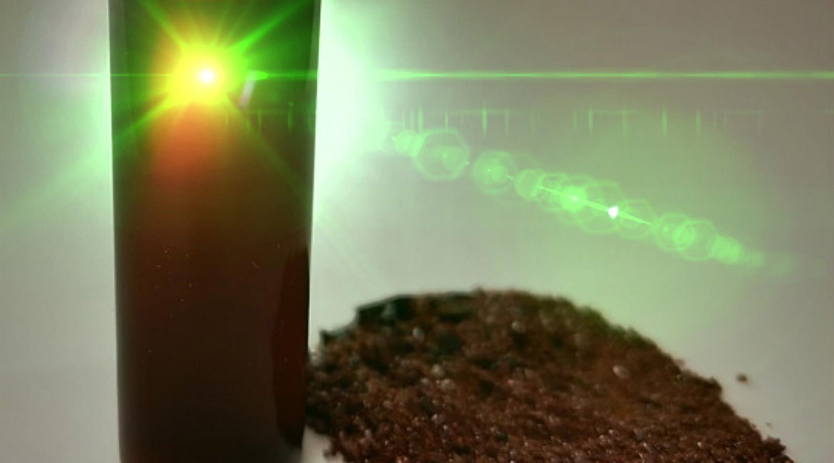
 Such high temperature requirements make these materials difficult candidates for additive manufacturing applications. In the NOMAD research group, directed by Professor Sylvain G. Cloutier in the Electrical Engineering Department at ÉTS, researchers found a way to produce defect-rich TiO2 that no longer requires high temperatures for processing. Instead, this new formulation allowed researchers to completely crystallize thin films of TiO2 using visible light in the form of focused lasers and high energy xenon lamps, all under ambient conditions, thus setting the stage for large area processing of this material using methods that are compatible with additive manufacturing [3,4] and production lines.
The Taming of TiO2 Crystallization
The two more common crystalline forms of TiO2 are called Anatase and Rutile. They are commonly found in nature and their synthesis is mutually exclusive under traditional chemical routes. With this new TiO2 formulation, both phases are easily obtained within the same thin film because the intensity of the light used for conversion can be adjusted to meet the energy requirements of each TiO2 polymorph without affecting previously crystallized areas.
In order to prove the potential of this new formulation in large area applications, researchers from NOMAD set out to test conversion capabilities using a low-cost laser-engraving system, part of a commercially available 3D printing system [6]. The cost of the blue-purple, 405 nm laser unit is under US$35, and all the conversion procedures were implemented using standard GCODE programs. This approach allowed the team to create complex patterns where areas of anatase, rutile and amorphous TiO2 existed side by side. These results are important because it shows that large area films, of various square centimetres, can be readily crystallized on-demand using common processing techniques and under normal environmental conditions.

Figure 3. (a) Geometric pattern showing the presence of amorphous, anatase and rutile TiO2. (b) Micrograph 3D reconstruction of the converted areas next to one another. A – anatase, R – rutile, Am – amorphous.
Applications that Will Benefit from this Research
One of the main uses of TiO2 is in photocatalytic applications, where the material reacts to UV light present in sun rays or artificial sources to break down pollutants in water and air. This serves an important purpose in agriculture and water treatment plants. It has been proven that a combination of TiO2 phases, co-existing side by side in thin films improves the capabilities of a photocatalytic system compared to a system made only of a single TiO2 polymorph. Fabricating such a film using our TiO2 formulation, in the form of an ink [7] paves the way, for the first time, to creating such devices using printed electronic-compatible manufacturing techniques.
The ability to crystallize large areas of TiO2 thin films using inexpensive conventional laser treatment machines, as the researchers proved in their publication [6], opens up important possibilities and surpasses current technological challenges and limitations. Indeed, optoelectronic devices, such as transparent flexible solar cells and flexible sensors are fabricated using several layers of different materials and substrates which are very sensitive to high temperatures and can be easily destroyed by traditional TiO2 processing temperatures. In the past, these high-energy annealing requirements prevented TiO2 use in flexible optoelectronic applications. Nowadays, our ability to crystallize TiO2 locally, using low-cost light sources and short processing times, while preventing damage to other substrates and materials finally allows the inclusion of this elusive material in production lines.
Additional Information
For more information on this research, please read the following research paper: Gerlein, Luis Felipe; Benavides-Guerrero, Jaime Alberto; Cloutier, Sylvain G. 2019. Laser‐Assisted, Large‐Area Selective Crystallization and Patterning of Titanium Dioxide Polymorphs. Advanced Engineering Materials. 191014.