Creating More Efficient Thermoelectric Devices

The header image was purchased on Istock.com and is protected by copyright.
By converting heat loss into electricity, thermoelectric technology has the ability to improve the energy efficiency of most electrical appliances. Modifying thermoelectric material properties at the nanoscale helps increase their performance, yielding better energy recovery. These structural modifications and the use of masks allow us to present an easily produced device that is compact and powerful.
A Brief History
Discovered at the beginning of the 19th century in Europe by Seebeck and Peltier, thermoelectricity is still a current field of research, offering interesting perspectives. Experiments led this researcher and watchmaker to highlight the Seebeck and Peltier effects. Seebeck noted that a difference in electrical potential is produced with the junction of two different materials at different temperatures—the Seebeck effect. This phenomenon makes it possible to generate electricity by applying a temperature gradient. Peltier meanwhile, observed that heat is produced and absorbed at the junctions between materials following the directional flow of the applied current. The Peltier effect reduces the need for coolant gases for example, known to be harmful to the environment.
Here, we will focus on the Seebeck effect that transforms a temperature gradient into electricity. In light of the recent awareness of our growing energy consumption and the resulting impact on the planet, the Seebeck effect offers the added advantage of increasing energy efficiency while reducing waste. In the United States alone, half of the energy produced is lost as heat [1]. However, if we consider heat sources from combustion engines or electronic devices, the potential applications of thermoelectricity in our daily lives then present infinite possibilities! We already use this physical phenomenon, be it in electric coolers (Peltier effect), or with the well-known Voyager 1 and 2 probes, which are still sending signals to Earth [2] 40 years after their launch.
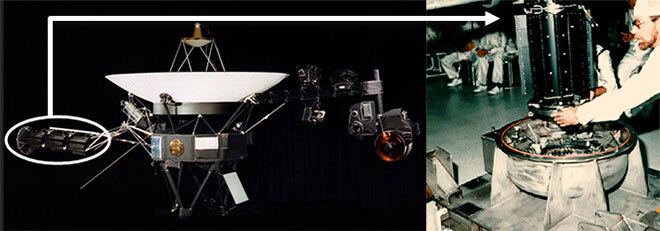
Figure 1 – Photo of a Voyager probe on the left and a thermoelectric device on the right
Manufacturing Thermoelectric Devices Using Pulsed Laser Deposition
The technological advances of the last decades and the increased computing power of computers have revealed that the most interesting performances of thermoelectric materials are found within thin layers at the nano- or even micrometer scale. Unlike so-called “massive” materials, at these scales it is possible to influence the structure and positioning of atoms. Pulsed laser deposition is used to obtain a highly accurate control over the structure of deposited layers. The laser emits very high energy pulses over very short time intervals to a target on the deposited material. The target is first placed in a very high-vacuum chamber, see Figure 2. The laser pulses then deposit material in plasma form and eject a plume of material perpendicular to the target.
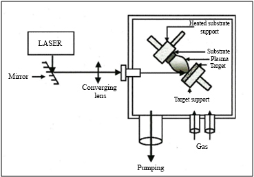
Figure 2 – Diagram of a pulsed laser deposition system
Depending on the parameters used, this plume will then condense on a substrate placed parallel to the target. The type of laser, number of pulses, substrate temperature or pressure inside the chamber are all interrelated parameters to take into account. Even today, not all light-matter interactions are fully understood and are still being debated.
A Compact and Powerful Device
As part of our study, we plan to use the heat loss of electronic devices and achieve energy recovery using low temperature gradients (between 5 ° C to 80 ° C). The manufacturing method of our planar devices is relatively simple: it is based on three masks with micrometric openings arranged on a glass slide (see Figure 3). First, metal contacts must be deposited to supply electrical conduction within the device. A gold deposit of several hundred nanometers is achieved through thermal evaporation. Then, two masks are used successively to deposit lines of thermoelectric materials. The use of masks is both simple and effective and can produce energy recovery devices at lower costs than those achieved by etching or lithography.
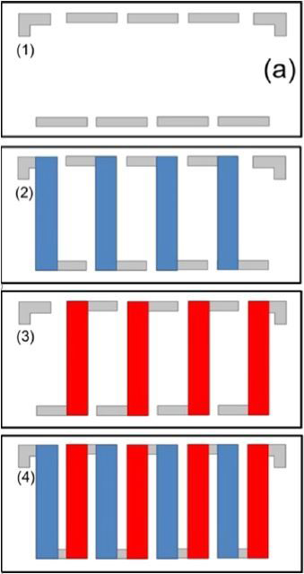
Figure 3 – Diagram of masks and depositions shown in this study
In addition to using masks, it has been possible to produce thermoelectric devices offering better energy recovery than those with a similar geometry previously reported in the literature. These results are all the more interesting considering the substrate temperature during deposition: they were done at 45 ° C instead of the 200 ° C and 300 ° C usually required. The final advantage is that no gas in the chamber or annealing was used after deposition. These characteristics have special benefits because they result in a considerable reduction in the complexity, the cost of production and the thermal budget required to create these devices. These results were possible thanks to a highly accurate control of deposition on the target. As reported, it is above all with respect to stoichiometry (proportion of each chemical element) at 45 ° C that these unparalleled performances can be confirmed.
Conclusion and Outlook
Following the publication of these findings, we hope to encourage researchers to continue the work to gain a better understanding of this phenomenon. We also wish to pave the way for the design of simplified, compact and efficient thermoelectric devices. With these devices, we hope to optimize the energy efficiency of our electrical appliances by converting heat loss into electricity.
Additional Information
For more information on this research, please refer to the following paper: Fourmont, P.; Gerlein, L.F.; Fortier, F.-X.; Cloutier, S.G.; Nechache, R. 2018. “Highly Efficient Thermoelectric Microgenerators Using Nearly Room Temperature Pulsed Laser Deposition”. ACS Applied Materials & Interfaces. 10 (12), pp. 10194-10201.