Characterizing Electro Optic Thin-Film Materials by Terahertz Images
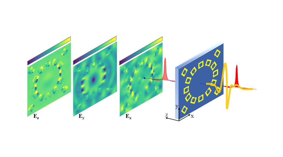
Image from the authors. CC Licence.
Electro optic (EO) thin-film plays an important role in the future of the integrated circuit industry, particularly in information technology where high processing efficiency is required. Currently, characterizing the EO coefficients of this material is very challenging due to its slim thickness. Our objective is to introduce a method to help solve this problem. Our method allows pinpointing thin-film EO coefficients through electric field images in the terahertz (THz) frequency range.
Introduction
Today, our lives are increasingly dependent on information technologies for communication, computing, and sensing. We demand smaller and smaller devices with higher speeds and lower costs. To develop such devices—especially in new generations of integrated circuits—we require advanced materials suitable for these technologies. EO thin-film plays a significant role in achieving this goal. Thin-film production for such device purposes has been proposed over the past 50 years. But characterizing this thin-film material remains challenging because of their thinness. In this work, we propose a new method to characterize this material using THz microscopy.
Thin-Films and their Application
A thin-film is known as a layer of material with a thickness ranging from nanometres to micrometres (Figure. 1 [a]). Lithium niobate (LiNbO3) is the most common material for this task. The cost of thin-film is relatively low compared with the corresponding bulk material as it performs the same functions in surface processing or guided light waves.
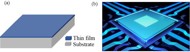
Figure 1 (a) thin-film layer on a substrate, and (b) using thin-film in EO devices.
Crystal thin-films play an important role in developing materials with new and unique properties for various applications. For example, thin-films with electro-optic (EO) properties are widely used for advanced communication and computing systems. Specifically, they are used for different functions like modulators, switches, and attenuators in EO devices [1,2] (Figure. 1 [b]).
In short, an EO thin-film is the interface that converts electrical information to light information and vice versa. This ability is essential in meeting the immense demand for ever-faster digital communication. Consequently, finding novel thin-film materials with better performances will directly help process information faster and more accurately.
The Challenges of EO Thin-Film Characterization
In general, optical properties of EO materials change in response to an applied electric field. This results in a modulation of the optical beam polarization that simultaneously passes through the material. The EO properties of these materials are usually characterized by applying an electric field in different directions. Concurrently, an optical beam passes through them to measure EO responses. It is important to mention that there are different responses from an EO material according to its x-, y-, and z directions. Typically, applying an electric field to reveal all EO responses requires several electrodes to be placed on the material in different orientations. While placing electrodes on bulky materials is a straightforward procedure, it is very challenging with thin-film materials. Moreover, since thin-films are normally thinner than, or comparable to, the wavelength of light, the interaction range with light propagating through is also limited. This restriction considerably reduces the sensitivity of the characterization method. Thus, new solutions for thin-film characterization still need to be demonstrated.
The Proposed Solution: A Split-Ring Resonator
To overcome the loss of sensitivity due to the slim thickness of thin-films, we first increased the amplitude of the applied electric field on the thin-film to enhance the interaction inside the material by generating intense THz pulses [3]. Second, we designed and introduced an artificial material to catch the electromagnetic radiation in the THz frequency range (a metamaterial called a Split-Ring Resonator [SRR]). The SRR acts as a tiny antenna that can easily be designed by an engineer. Once excited by a THz pulse, the resonant responses of our SRR function as an electrode that simultaneously probes the thin-film responses in all directions, as illustrated in Figure. 2 (a). In order to reveal the electro-optic responses from a thin-film material, we visualized in time and in space the electric field distribution on the SRR using a THz microscopy method, as shown in Figure. 2 (b).

Figure 2 (a) different electric field components on a single SRR antenna, and (b) spatial distribution of the resonant electric field for Ex, Ey, and Ez.
Terahertz Microscopy
It is well known that visible microscopy allows to observe the properties of an object that cannot be seen with the naked eye. High spatial resolution is achieved through subwavelength imaging capability. Commonly, for visible microscopy methods, measurements provide images of light intensity. For THz microscopy methods, a direct reading of the amplitude and phase information of the electric field is routinely done [4]. This capability allows to record the various electromagnetic field responses of a metamaterial not only in space, but also in the time domain. Therefore, we can observe the 3-dimensional electric field responses from an antenna (SRR) placed on a thin-film material with their distinctive orientation. As illustrated in Figure 3, this method is used to reveal EO responses of a thin-film material through electric field images, where the unique components for x-, y-, and z-directions are spatially and temporally discriminated.
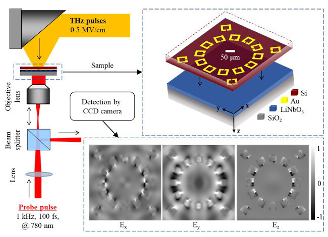
Figure 3 THz microscopy of EO thin-film with SRR on top.
Revealing Electric Field Responses of an EO Thin-Film
Figures 4 (a) and (b) show the electric field responses of the antenna on LiNbO3 thin-film using THz microscopy and simulation, respectively. The simulation results are considered as reference electric field responses (Ex, Ey and Ez) from SRR on the thin-film in x-, y-, and z direction. Here, our experimental result shows that the response of SRRs on LiNbO3 films corresponds with the response in y-direction. Therefore, knowing the crystallographic structure of the thin-film material under investigation renders the absolute value of the corresponding EO coefficient accessible [5].
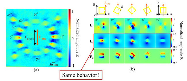
Figure 4 (a) experimental result at 0.5 THz, and (b) simulated electric field response.
Conclusion
Our results show that THz microscopy is a proper method to reveal all EO responses in x-, y-, and z-directions of thin-film EO materials. Here, the 3D electric field responses were performed using SRR on the well-known LiNbO3 thin-film crystal. In principle, we should be able to retrieve the EO components of an unknown material following this demonstration. Ultimately, since the SRR structure also exhibits a magnetic response (shown in Figure. 5), this method could be extended to characterize novel magneto-optic materials.
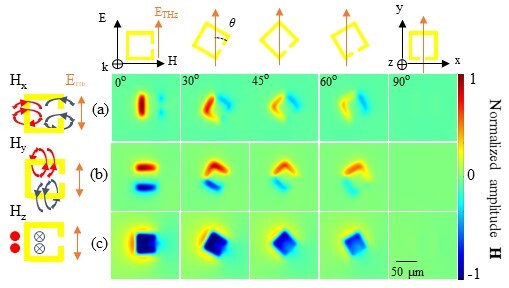
Figure 5 simulated magnetic response from SRR in (a) x-, (b) y-, and (c) z-directions.
Additional Information
For more information on this research, please read the following paper:
Amirkhan, F.; Sakata, R.; Takiguchi, K.; Arikawa, T.; Ozaki, T.; Tanaka, K.; Blanchard F. 2019. “Characterization of thin-film optical properties by THz near-field imaging method”. Journal of the Optical Society of America B. Vol. 36, issue 9, pp. 2593-2601.